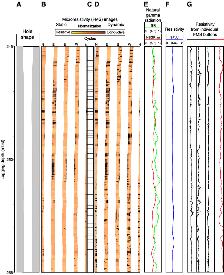
Figure F42. Formation MicroScanner (FMS) images and conductive layers between 245 and 255 mbsf showing (A) hole shape, (B) static and (D) dynamic (window height = 0.5 m) normalization of the microresistivity images, (C) conspicuous conductive layers, (E) total gamma radiation (HSGR from HNGS and gamma radiation [GR] from MGT) and (F) shallow resistivity (SFLU) logs, and (G) extracted FMS button records showing the poor pad/formation contact (red).